キーワード: 太陽電池、薄膜、豊富な元素、省資源、省エネルギー、バリウムシリサイド
http://www.bk.tsukuba.ac.jp/~ecology/index.html
 このユニットの母体となる研究室は、技術をステップアップしつつ、つねに新しい対象にチャレンジしてきています。「分子線エピタキシー(MBE)による金属/ 絶縁体積層構造の結晶成長と共鳴トンネルトランジスタの研究」から「MBE による半導体鉄シリサイド(β-FeSi2)の結晶成長と赤外発光デバイス」へ。次には「シリコンベース半導体レーザ」へ。また「半導体シリサイドBaSi2 をベースとする高効率薄膜太陽電池に関する結晶成長とデバイス化」にテーマが変遷しています。いずれも、私たちの周囲に大量にあり、かつ安全な元素で高機能デバイスを作り上げようとするポリシーが感じ取れます。
バリウムシリサイド系高効率薄膜太陽電池の研究開発
本リサーチユニットでは、化学的に安定、かつ薄膜にすることでの原料の少量化が可能であり、また光劣化のない高効率薄膜太陽電池の研究を進めています。一例として、図1 のようにBaSi2結晶薄膜のpn 接合による太陽電池の研究開発も進めています。n 型BaSi2 結晶薄膜をSi (111)基板上にMBE で形成し、レーザードーピング法によりB(ホウ素)を注入することでp 型に変換してpn 接合をつくるものです。(Jpn. J. Appl. Phys., 2004)さらに、自然酸化膜を介してBaSi2 結晶薄膜上にMo 酸化膜、ITO(酸化インジウムスズ)透明電極層を形成して太陽電池性能を評価しました。(図2、Appl. Phys.Lett., 2015)非常に明瞭なショットキー特性を示すとともに、可視光全域(波長:約400 – 800 nm)で、逆方向バイアス印加時にバイアスのない状態に較べて30 倍程度外部量子効率が高くなることが分かりました。将来は、単結晶シリコン太陽電池と同程度以上の変換効率を目指しています。
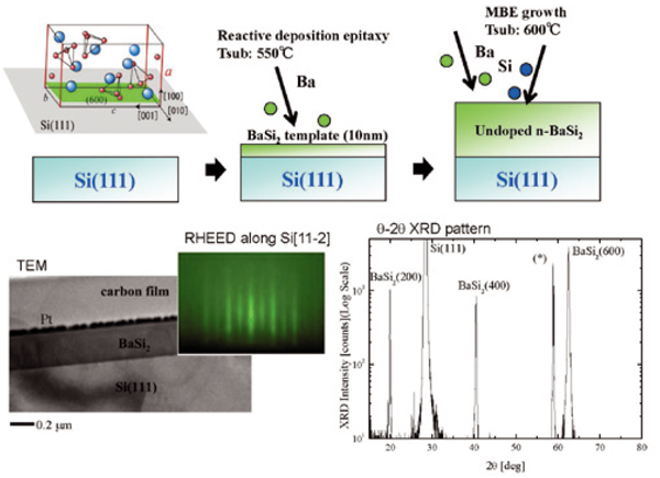
図1:Si 基板上へのBaSi2 成長の原理と反射高速電子線回折(RHEED)による面内結晶性評価
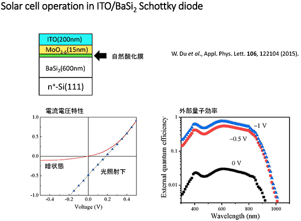
図2:BaSi2 膜を使った太陽電池の例
研究は国内外の連携で!
本リサーチユニットは多くが筑波大学の研究者で構成されています。しかし、研究を加速して、より高度な成果を得るためには国内外の連携が重要と考えています。物質・材料研究機構とはカソードルミネッセンス(CL)による材料評価、シュトゥットガルト大学とはレーザードーピング法について共同研究を進めています。また、つくばイノベーションアリーナ(TIA-nano)のナノエレクトロニクス研究コアを通じて産業技術総合研究所とも連携しています。さらには、名古屋大学との連携、放射光施設(SPring-8)の利用の他に実用化を目指して企業との共同研究も行っています。
社会への貢献・実績
● 書籍による成果普及:「シリサイド系半導体の科学と技術: 資源・環境時代の新しい半導
体と関連物質」(裳華房、2014、前田 佳均 編集)で反応性エピタキシャル成長、Ba シ
リサイド、シリサイド発光素子/ 太陽電池に関する紹介
● 産業技術総合研究所(AIST)や物質・材料研究機構(NIMS)などで活躍する太陽電池
研究者との連携強化とつくば連携による研究推進
● 幅広い視野を持った次世代リーダーとなる若手研究者の育成
● 筑波大学公開講座「日本の技術と北アフリカの太陽光と砂で世界の電力問題に挑む」
−太陽電池を薄く作る試み− 2014 年10 月3 日、筑波大学
取材:平成27年3月25日
Development of photonics and spintronics devices through utilization of abundantly available elements - Sustainable electronics
Unit name: High-Efficiency Thin-Film Solar Cells
Key words: solar cell, thin film, abundant element, energy saving, barium silicide
The laboratories serving as the base for this unit have always been making efforts for technical advancement and development of new objects. The research theme has been shifted from “research on crystal growth of metal/insulator layered structure by molecular beam epitaxy (MBE) and resonant tunneling transistors” to “semiconductor iron silicide (β-FeSi2) crystal growth by MBE and infrared light-emitting device”, “silicon-based semiconductor laser” and then to “crystal growth related to semiconducting BaSi2-based high efficiency thin-film solar cells and device development.” Each of these themes reflects the policy of creating high-function devices from safe elements abundantly available around us.
R&D on barium silicide-based high efficiency thin-film solar cells
At this research unit, research has been ongoing on high efficiency thin-film solar cells which are chemically stable, allow saving of raw materials by adoption of the thin film form which are free of photodegradation. For example, R&D is now under way on a solar cell composed of a BaSi2 pn junction diode as shown in Fig. 1. With this technique, n type BaSi2 crystal film is formed in a Si (111) substrate by MBE, followed by doping of boron (B) by laser doping to convert it into p type and to create a pn junction diode (Jpn. J. Appl. Phys., 2004). Furthermore, Mo oxide membrane and transparent ITO (tin-doped indium oxide) electrode layer were formed on the BaSi2 crystal film via a naturally oxidized membrane, and the performance as a solar cell was evaluated (Fig. 2, Appl. Phys. Lett., 2015). Rectifying current voltage characteristics were obtained and the the external quantum efficiency was increased by 30 times by a bias voltage. The efficiency of 9.9% was achieved in p-BaSi2/n-Si solar cells (Appl. Phys. Lett. 109, 072103 (2016)). The ultimate goal of this research is to achieve a conversion efficiency of 35% in a BaSi2-pn/Si-pn tandem structure solar cell.
Fig. 1: Principle of BaSi2 growth on board and evaluation of in-plane crystallization by reflection high energy electron diffraction (RHEED)
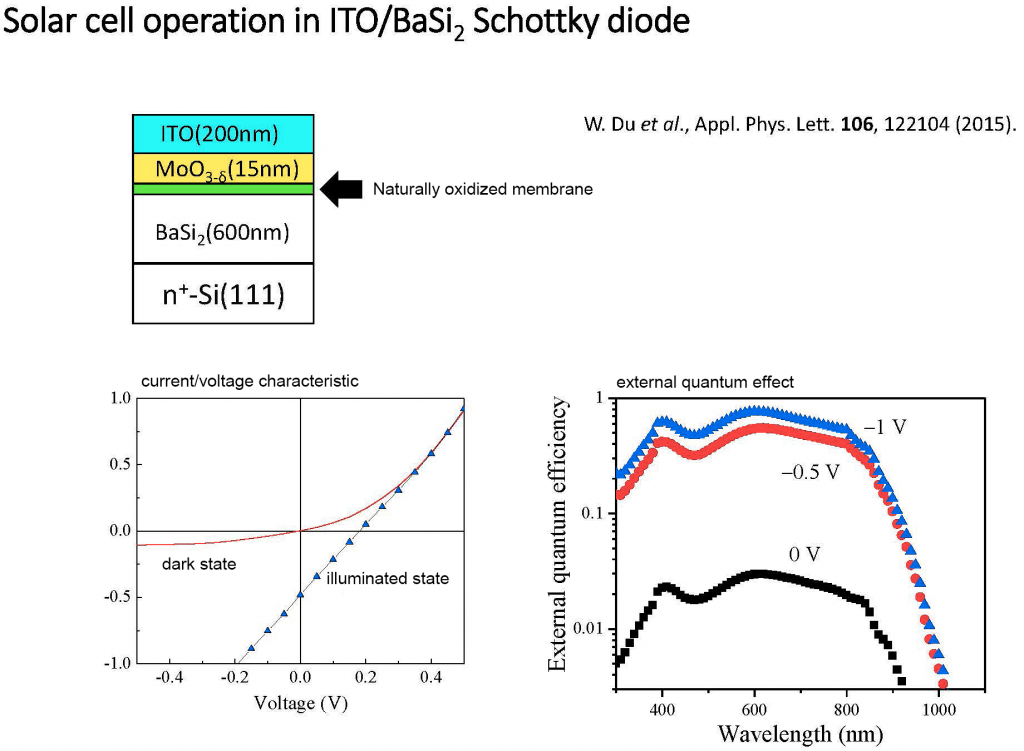
Fig. 2: Example of solar cell using BaSi2 film
Domestic and overseas linkage in research!
Many of the members of this research unit are researchers at the University of Tsukuba. However, to accelerate the research to get higher outcomes, we think domestic and overseas linkage is important. Joint research is now underway with the National Institute of Materials Science concerning evaluation of materials by cathode luminescence (CL) and with Stuttgart University over the laser doping technique. Furthermore, via the Nanoelectronics Research Core of the Tsukuba Innovation Arena (TIA-nano), we are linked to the National Institute of Advanced Industrial Science and Technology. Furthermore, we have linkage to Nagoya University, are utilizing the Synchrotron Radiation Facility (SPring-8), and are conducting joint research with enterprises on commercialization of new technologies.
Social contributions and achievements
– Dissemination of outcome via publication of books: “Science and technology on silicide-based semiconductors: New semiconductors and related materials in the age of resources and environments” (edited by Yoshihito Maeda, Shokabo, 2014), introducing reactive epitaxial growth, barium silicide and silicide-based light-emitting elements/solar cells.
– Reinforcement of linkage to solar cell researchers working at the National Institute of Advanced Industrial Science and Technology (AIST), National Institute of Materials Science (NIMS), etc., and promotion of research through the Tsukuba Research Core.
– Cultivation of young researchers with wide perspectives serving as the next-generation of leaders.
– University of Tsukuba Open Seminar “Challenging the Global Issue of Electric Power Shortage by Japanese Technology and North African Sunlight and Sand” — Attempts of creating thin solar cells — October 3, 2014, University of Tsukuba.
Interviewed on June 5, 2015