他のメンバー : 桑原 純平 川島 英久 石井 宏幸 金澤 研 前島 展也 藤岡 淳 所 裕子 木島 正志 神原 貴樹 松石 清人 日野 健一
他機関 : 福島 大介 小暮 希望 岡野 和史 北澤 正広 梶 弘典 竹谷 純一 尾坂 格 若宮 淳志 小野 新平
キーワード:オペランドスピン解析、有機無機材料、有機無機デバイス、物性、機能
http://www.ims.tsukuba.ac.jp/~marumoto_lab/index.html
 有機半導体材料を用いた有機デバイス(有機ELディスプレイなど)は、軽量・フレキシブルな次世代デバイスとして注目されています。従来は、材料となる有機無機半導体やそのデバイスの技術開発に、マクロスケール特性観察に基づく試行錯誤でしか取り組めなかったため、研究開発時の費用・時間を削減する方策が求められていました。
有機無機スピンエレクトロニクス・リサーチユニットは、電子スピン共鳴(ESR)分光を始めとするミクロ解析技術と理論計算、有機・無機の材料合成、マクロ解析技術とデバイス作製を包含する異分野融合チームにより、高機能・高効率な次世代デバイスの開発拠点を実現しています。
世界初のミクロ解析技術で有機無機デバイスの材料費・開発コストの低減へ
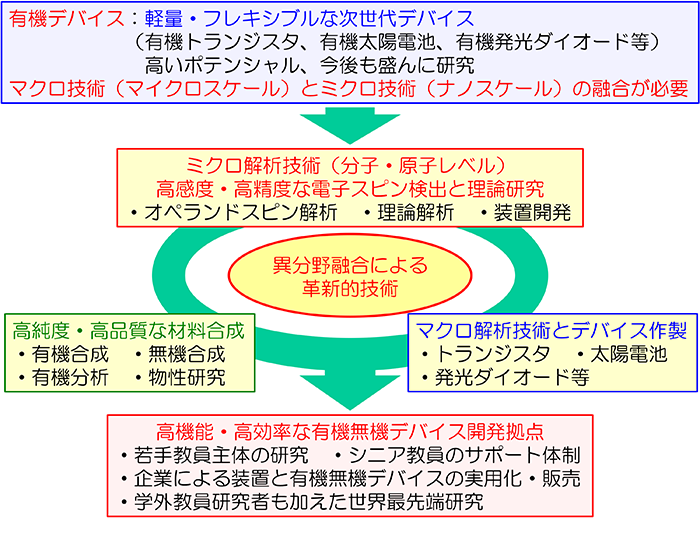
図1:有機無機デバイス開発拠点形成の概念図
当リサーチユニットでは3つの異分野を融合し、連携しながら研究を進めています。1つ目は、有機無機スピンエレクトロニクス・デバイスのミクロ解析をする「ミクロ解析技術」、2つ目はデバイスを作製するための材料を合成する「材料合成」、3つ目はミクロ解析技術で明らかにした情報と材料を用いて、実際にデバイスを作製し評価する「マクロ解析技術とデバイス作製」です。
これまでの研究では、3つ目の「マクロ解析技術とデバイス作製」に相当する伝導・発電・発光等のマクロ解析技術を用いた物質解析や、デバイス構造の研究とそれに基づくデバイス作製技術が主でした。そのため、マクロスコピックな有機無機スピンエレクトロニクス・デバイスの振舞いは明らかにできても、ミクロスコピックな振舞いについては暗中模索的開発を強いられていました。
当リサーチユニットが世界で初めて開発したミクロ解析技術は、より戦略的なデバイス開発を可能にし、研究開発コストを抑え、開発のスピードアップを可能にしました。有機トランジスタ、有機太陽電池、有機LEDなどの有機無機スピンエレクトロニクスを用いたデバイスの効率的量産・軽量化、さらには低価格化が期待されています。
産学連携チームで企業と学生の双方に相乗効果を創出
学外研究者と学生の研究を通じた交流
当リサーチユニットの研究では、オペランドスピン解析や理論解析による分子・原子レベルのミクロ解析技術も活用しながら、有機無機材料やそのデバイスの解析の深化を目指しています。
研究を進める際、企業と連携することによって、既存の製品の性能向上や商品開発にダイレクトに作用することも、当リサーチユニットの価値のひとつといえます。将来的には壁やブラインドに貼り付けられる太陽電池の開発や、液晶以上に解像度の高いディスプレイの普及など、人々の生活や市場に直結する技術を革新していきたいと考えています。
また、理論、実験、素材という3つの異分野の第一人者(企業研究者を含む)と連携して研究を進めることは、学生への教育面にも寄与しています。たとえば、学生たちも携わるミクロ解析技術については、他の研究機関では行われていないため、リサーチユニット内の他のメンバーから意見を求められるシーンも多々あります。第一線で活躍する研究所や装置メーカーの研究者、他大学の教授などに、いわば「指導する」ことは、学生たちにとって大変貴重な経験になっているようです。
このように、当リサーチユニットの活動を通じ、企業と学生の双方への相乗効果による研究促進と、社会に対する実益をもたらしていきたいと考えています。
社会への貢献・実績
- 次世代高輝度有機発光デバイスのミクロ解析と高特性素子開発(2019年)
- 筑波大学リサーチユニット強化事業採択による高機能・高性能な有機無機スピンエレクトロニクスの研究開発拠点形成(2019年)
- 第1回有機無機スピンエレクトロニクス研究会の開催(2020年)
- 大学院生の第4回フロンティア太陽電池セミナー優秀ポスター賞の受賞(2019年)
- 大学院生の筑波大学数理物質科学研究科修士論文発表優秀賞の受賞(2019年、2020年)
取材日:2020年1月29日
Contributing to spread of next-generation device through micro analysis
Unit members : Kuwabara, Junpei Kawashima, Hidehisa Ishii, Hiroyuki Kanazawa, Ken Maeshima, Nobuya Fujioka, Jun Tokoro, Hiroko Kijima, Masashi Kanbara, Takaki Matsuishi, Kiyoto Hino, Ken-ichi
Other agencies : Fukushima, Daisuke Kogure, Nozomi Okano, Masahito Kitazawa, Masahiro Kaji, Hironori Takeya, Junichi Osaka, Itaru Wakamiya, Atsushi Ono, Shimpei
Unit name: Organic-Inorganic Spin Electronics
Key words: Operando spin analysis, Organic-inorganic materials, Organic-inorganic devices, Physical properties, Functions
http://www.ims.tsukuba.ac.jp/~marumoto_lab/index-e.html
Organic devices using organic semiconductor materials (such as organic EL display) are attracting attention as a lightweight flexible next-generation device. Measures to reduce the cost and time of research and development have been needed because previously, the technological development of organic-inorganic semiconductors serving as a material and devices thereof could be coped with only by trial and error based on the observation of macro-scale characteristics.
Organic-Inorganic Spin Electronics Research Unit realizes a development base of high-function high-efficiency next-generation devices by interdisciplinary team through micro analysis technology and theoretical calculation including electron spin resonance (ESR) spectroscopy, organic-inorganic material synthesis, and macro analysis technology and device preparation.
Toward reduction of the cost of materials and development of organic-inorganic devices using micro analysis technology first in the world
Fig. 1: Concept of base formation for organic-inorganic device development
Our Research Unit proceeds studies by fusing and cooperating with 3 different fields: first, ‘micro analysis technology’ performing micro analysis of organic-inorganic spin electronics/devices, second, ‘material synthesis’ synthesizing materials to prepare devices, and third, ‘macro analysis technology and device preparation’ actually preparing and evaluating a device using information and materials clarified by micro analysis technology.
In previous studies, substance analysis using macro analysis technology, such as conduction, power generation, and light-emitting, which corresponds to the third ‘macro analysis technology and device preparation’, and studies on device structures and device preparation technology based on these were mainly performed, so that although the behavior of macroscopic organic-inorganic spin electronics and devices could be clarified, development by grope in the dark was forced to be used to investigate microscopic behavior.
The micro analysis technology developed by our Research Unit first in the world enabled more strategic device development, suppressed the research and development cost, and increased the speed of development, so that efficient mass production, weight saving, and price reduction of devices using organic-inorganic spin electronics, such as organic transistors, organic solar cells, and organic LEDs, are expected.
Creation of synergistic effect for both companies and students through the industry-academia collaboration team
Exchange between outside researcher and student through research
Studies performed by our Research Unit aim at deepening analysis of organic-inorganic materials and their devices utilizing molecular/atomic-level micro analysis technology employing operando spin analysis and theoretical analysis.
Collaboration with companies in progressing studies directly acts on improvement of performance of existing products and product development and this is a value of our Research Unit. In the future, we want to innovate technology directly connected to people’s lives and markets, such as development of a solar cell attachable to walls and blinds and the use of a display with a resolution higher than that of liquid crystal.
In addition, progressing studies in cooperation with the leading persons of 3 different fields: theoretical, experimental, and material fields (including corporate researchers) contributes to student education. For example, since micro analysis technology in which students also take part is not performed at other research institutions, opinions are asked by other members of the Research Unit in many scenes. ‘Instructing’ institutions, researchers of device manufacturers, and professors of other universities active in the front lines seems to be very a valuable experience for students.
We are planning to promote research through the synergistic effect on both companies and students and bring actual benefits to society through the activities of our Research Unit as described above.
Social contributions and achievements
- Micro analysis of next-generation high-brightness organic light-emitting devices and development of high-performance devices (2019)
- Formation of research and development base of high-function, high-performance organic-inorganic spin electronics adopted for University of Tsukuba Research Unit Strengthening Project (2019)
- Holding of the first Organic-Inorganic Spin Electronics Study Meeting (2020)
- Winning of the excellent poster award at the 4th Frontier Solar Cell Seminar by a graduate student (2019)
- Winning of the award for excellent presentation of a master’s thesis by graduate students of Graduate School of Pure and Applied Sciences, University of Tsukuba (2019, 2020)
Interviewed on January 29, 2020